
Synopsys ($SNPS) Deep Dive
Designing the future of the semiconductor industry...


For years, Synopsys ($SNPS) and Cadence ($CDNS) have occupied some of the most valuable toll booths in the semiconductor industry.
Their software sits at the center of an increasingly complex chip-design process, their market positions have barely moved, and customers have had few credible alternatives. That combination has helped both companies command premium valuations for decades.
Then, almost overnight, the market began questioning the entire thesis…
Synopsys and Cadence had their own “DeepSeek moment” - similar to what NVIDIA and Broadcom experienced last year, when fears of cheaper and more efficient AI models wiped 15-20% from their market values in a single session.
The reaction from our community was almost immediate, with many readers asking for a deep dive now that the company was trading at a much more attractive valuation than it had historically.

Naturally, we decided to investigate - and here we’re.
Speaking of which, to join our chat, suggest future deep dives, participate in discussions, and receive daily updates, click the link below.
Exclusively available to paid subscribers.

The catalyst for the sell-off was Kimi K3, Moonshot AI’s newly released 2.8T parameter open-weight model. Since its weights are publicly available, developers can download, customize, and deploy it on their own infrastructure although running a model of this scale is certainly not free.
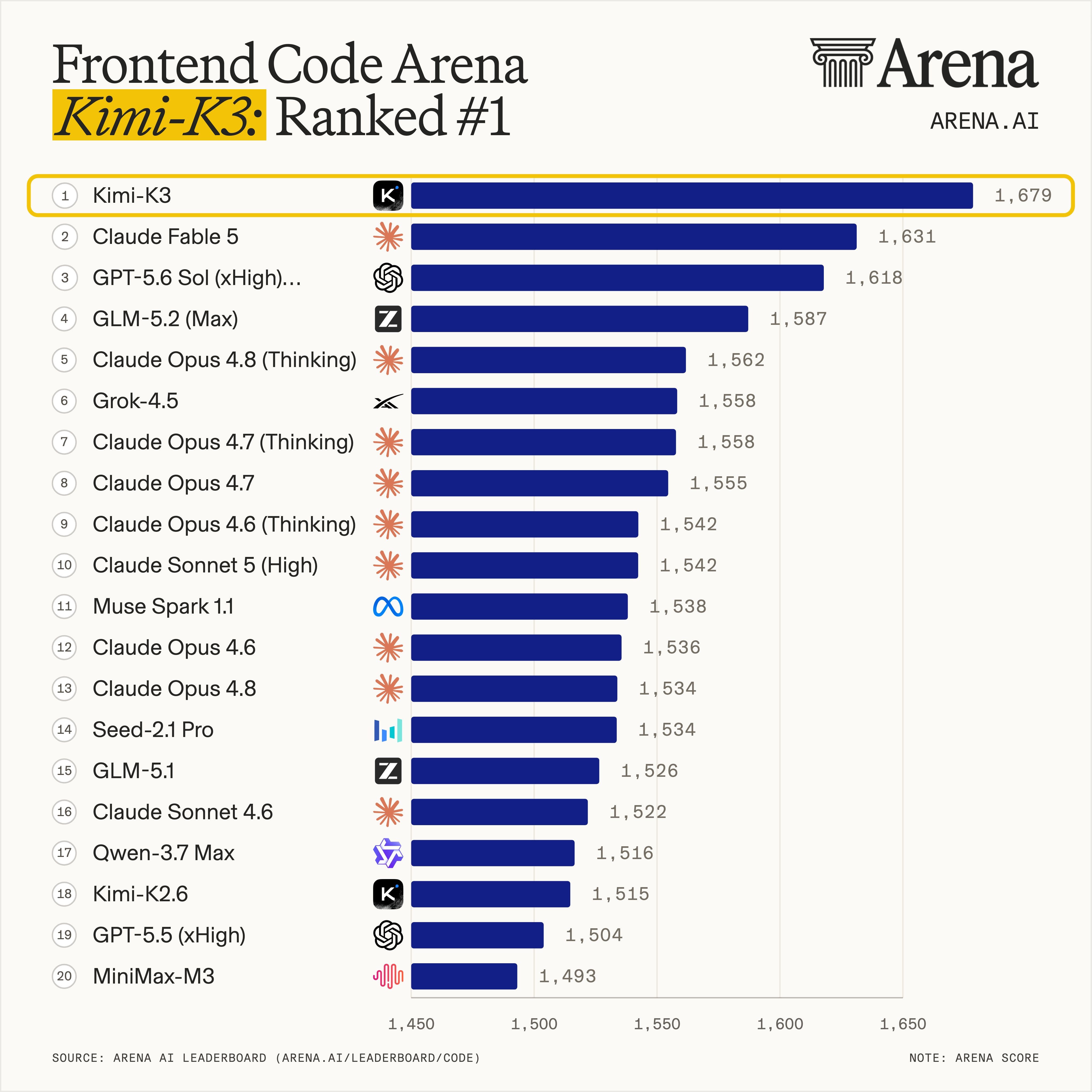
To demonstrate its ability to work autonomously through a complex, long-duration task, Moonshot asked K3 to design a chip and left it running for 48h with no human in the loop.
Using only free, open-source EDA tools and the Nangate 45nm academic library, the model designed, optimized, and verified a 4mm² chip layout that closed timing at 100MHz.
At no point did it use a Synopsys or Cadence product.
The market’s concern was easy to understand:
“If an openly available model can take a chip design from start to finish without paying the EDA vendors a cent, why should investors continue paying nearly 40x earnings for those vendors?”
Cadence and Synopsys shares immediately fell -9.5% and -7.8%, respectively.
Synopsys ($SNPS), which had already been on my watchlist for some time, became even more attractive after the sell-off - providing the catalyst for a much deeper investigation.
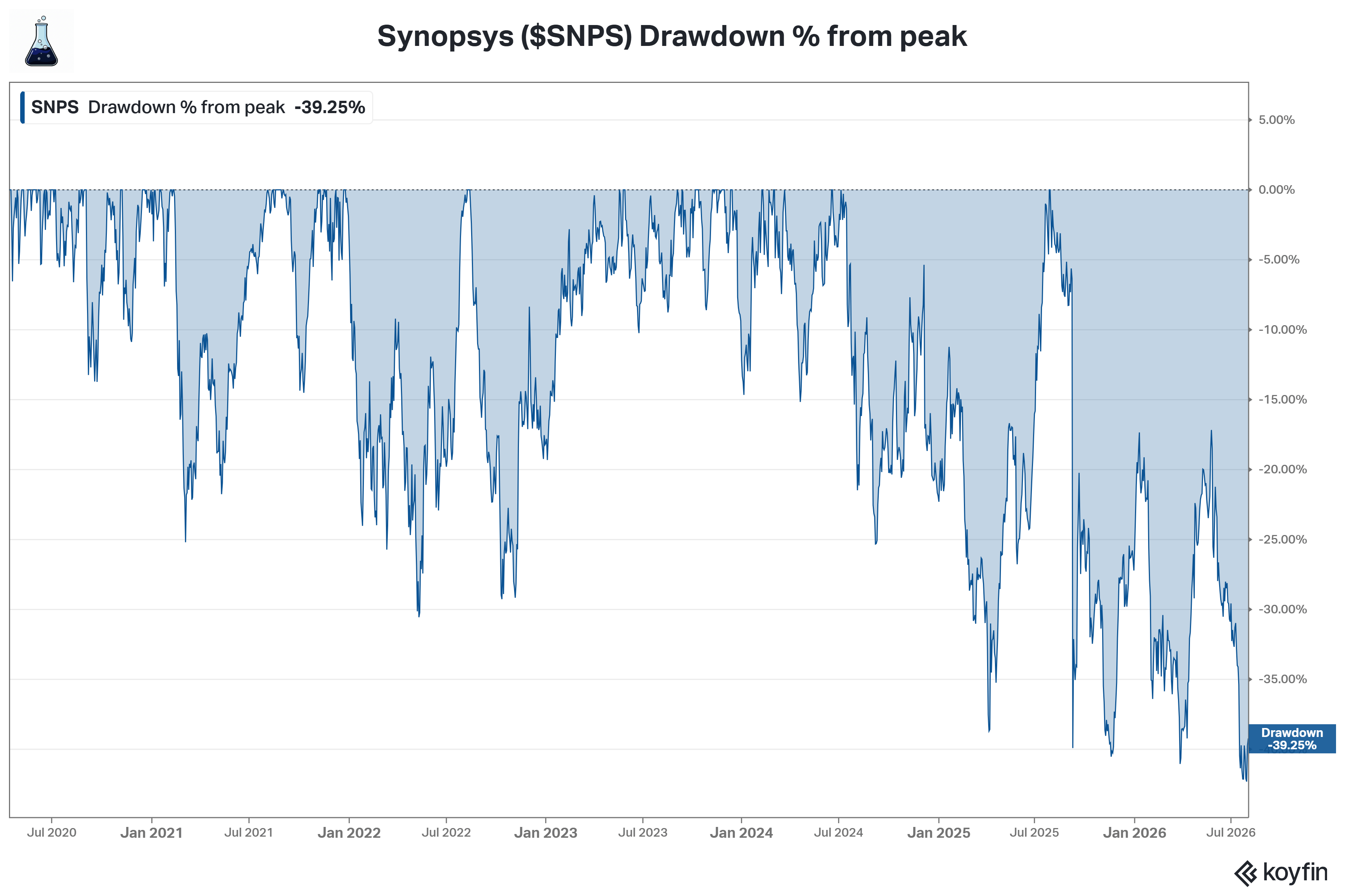
Was the market witnessing the beginning of EDA disruption?
Or had investors misunderstood what actually makes these businesses so difficult to replace?
That’s exactly what we’ll explore in this deep dive.
Table of Contents:
This deep dive is organized into the following sections:
EDA Industry Overview
Business History
Business Model
The Duopoly with Cadence
Ansys and Physical AI
The Design IP Business
Agentic AI
Kimi K3 and the Importance of PDKs
Competitive Advantages
Competitive Landscape
Capital Allocation and M&A
Growth Avenues and Backlog
Corporate Governance
Financials and Long-Term Targets
Valuation
Investment Thesis
Main Risks
Are We Buying $SNPS?
1. EDA Industry Overview:
What is EDA?
According to the definition on Synopsys’ own website:
“Electronic Design Automation (EDA) is a set of software and hardware tools that help engineers design and build electronic systems, especially computer chips (also called integrated circuits). EDA tools automate complex design tasks like planning, simulation, testing, and preparation for manufacturing. By using electronic design automation, engineers can create more advanced chips faster, reduce errors, improve power, performance, and area (PPA), and bring new products to market more quickly.”
Put more simply, EDA is a category of software, hardware, and services used to design, simulate, verify, and manufacture complex integrated circuits (or chips) and printed circuit boards (PCBs).
Yes, we are talking about an intersection between $IGV and $SOXX - and that may be precisely why EDA remains such an unfamiliar corner of the market for most investors.
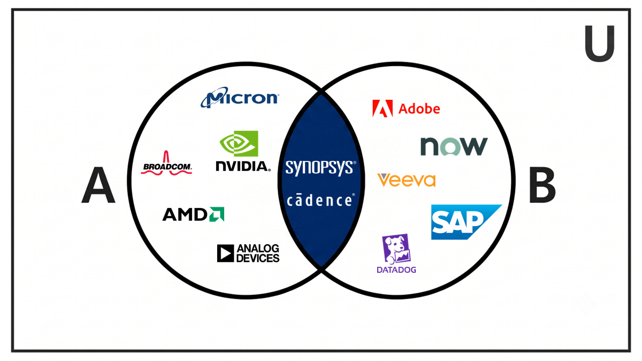
Its main functions include:
Automation: EDA tools automate repetitive and computationally intensive tasks.
Design Flow: EDA supports a structured design process, from the initial concept all the way to fabrication.
Verification: EDA tools provide simulation and verification capabilities that allow engineers to identify errors early in the development process.
Optimization: EDA helps optimize designs across several dimensions, including performance, power consumption, area, thermal management, and cost.
How large is the EDA industry?
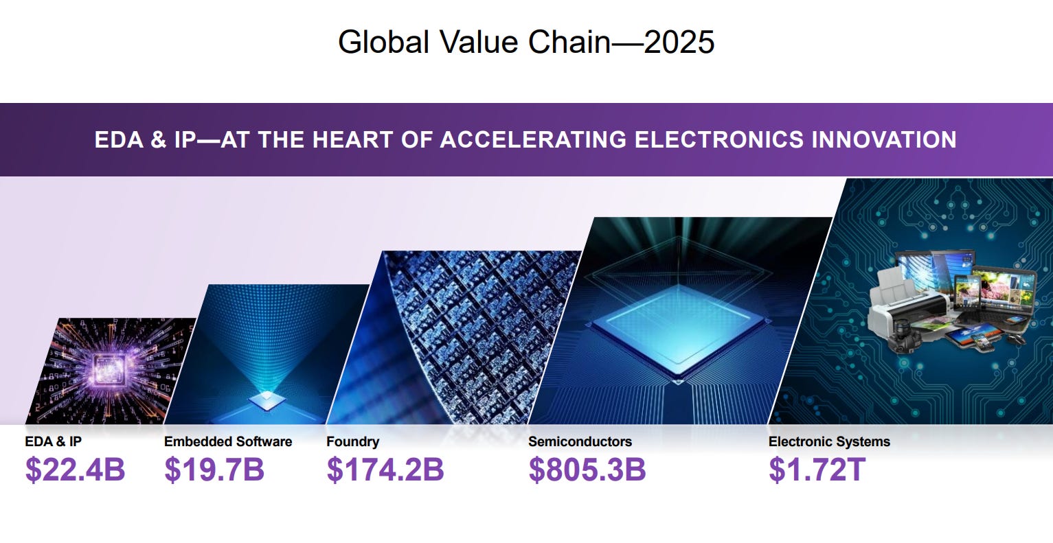
EDA and semiconductor IP together represent a market of ~$22B.
That relatively small layer enables around $174B in foundry revenue, which supports approximately $805B in semiconductor sales and, ultimately, about $1.7T in electronic systems.
EDA is the narrow neck of a very wide funnel: a small, high-margin toll booth that nearly everything downstream must pass through.
How EDA actually works?
A modern system-on-chip (SoC) can contain well over a billion transistors, each with features that are only a fraction of the width of a human hair. No individual - and no team of individuals - could design something of that complexity by hand. Well, at least not today...
In the early days of the semiconductor industry, during the 1960-1970s, electronic designs were created manually using paper, pencils, and basic drafting tools. Engineers selected logic gates by hand and connected them to build logic circuits.
But as integrated circuits became more complex and the number of components on each chip grew exponentially, these manual methods became increasingly time-consuming - and eventually completely inadequate.
It was in this context that EDA was born and gradually evolved into what it is today. Instead of designing every transistor and connection by hand, engineers describe what they want the chip to do and let software translate that intent into a manufacturable layout.
Electronic Design Automation is the software that performs this translation, verifies that the design works as intended, and ultimately signs it off for production.
Below is a look at the user interface seen by a semiconductor engineer using Cadence’s software, Synopsys’ main competitor:
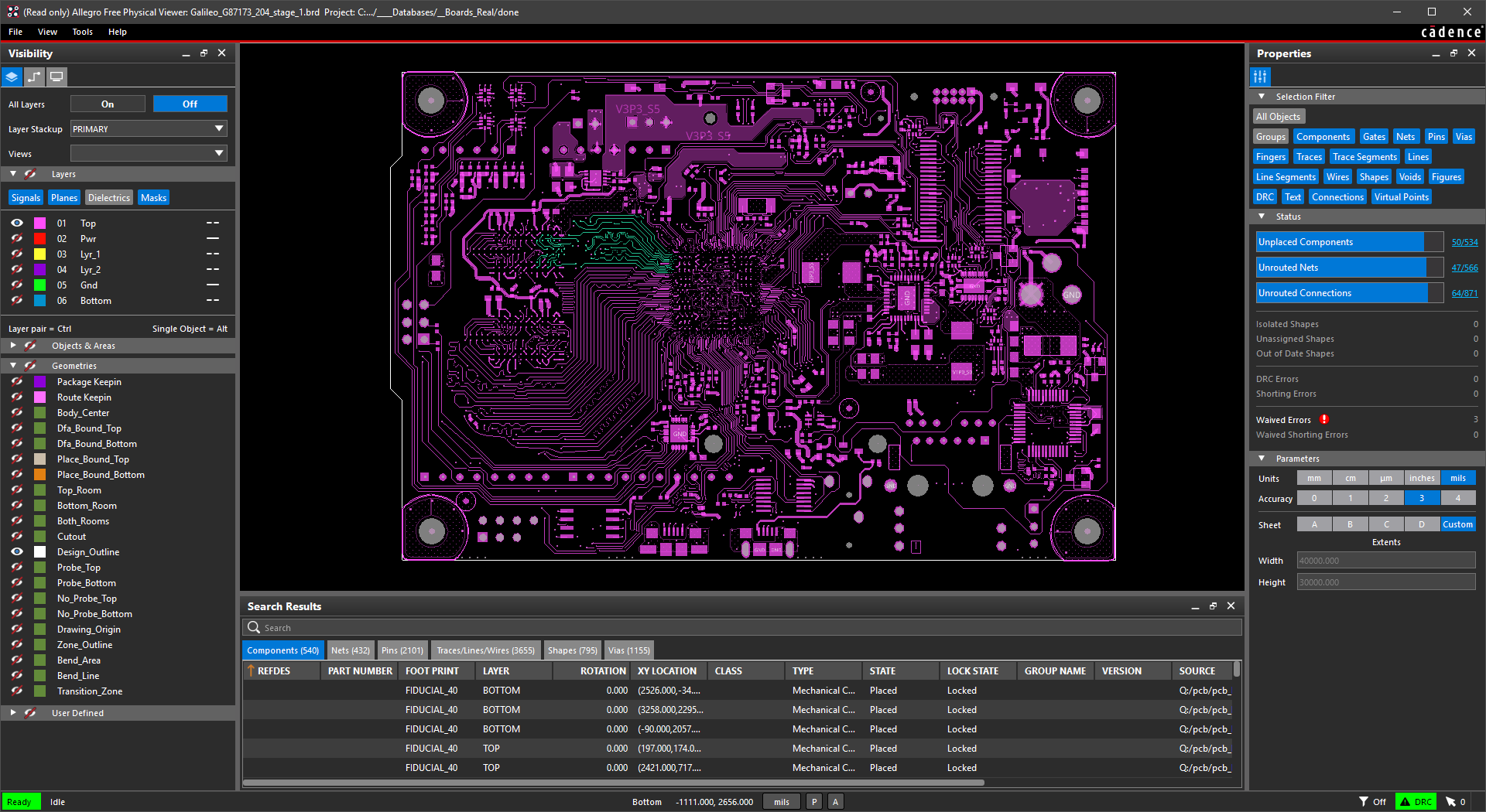
Designing a new chip is a long sequence of interconnected stages, each with its own tools, engineering teams, and potential points of failure.
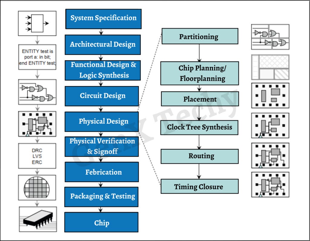
Broadly speaking, an engineer must go through the following steps:
Specification: every chip begins with a description of what it’s supposed to do. At this stage, engineers define its target performance, power consumption, physical area, functionality, and the interface standards it must support.
This is essentially the architecture phase, where the most important trade-offs are made. A chip can be faster, smaller, or more power-efficient - but rarely all three at once without additional cost or complexity.
RTL Design: once the architecture has been defined, engineers describe the chip’s logic using a hardware description language such as Verilog or VHDL.
This description is written at the register-transfer level, or RTL, which specifies how data moves between registers during each clock cycle. In practical terms, RTL is the closest equivalent to source code in software development. It’s the point at which the chip design becomes machine-readable.
Functional Verification: the next step is to make sure the RTL behaves as planned under a wide range of conditions.
Verification engineers create testbenches, write assertions, and run extensive simulation campaigns. Their objective is to find design flaws before the chip moves further into the development process, when errors become significantly more expensive to fix.
That’s also why verification is usually the longest and most resource-intensive stage of the entire design flow.
Logic Synthesis: after the RTL has been verified, synthesis software translates it into a gate-level netlist: a detailed representation of interconnected logic cells, such as AND gates, OR gates, and flip-flops - as shown in the image below.

Source: Fiveable, 2025. These cells are selected from a library designed for a specific manufacturing process.
In other words, this is the stage where an abstract description of the chip’s behavior begins to take the form of something that can eventually be manufactured. Curiously, it’s also the stage where Synopsys built its original franchise.
Physical Design: soon after, the gate-level design must be converted into a physical layout. The logic cells are placed across the silicon die and connected through layers of microscopic wiring - a process commonly known as place and route.
This is widely considered one of the most complex stages of the design flow because engineers must work around a long list of physical constraints. Signals must arrive at the right time, power consumption must remain within budget, heat must be controlled, and every component must fit within the available area.
Physical Verification and Signoff: before the design can be manufactured, the final layout must pass a large number of checks.
Engineers verify that it complies with the foundry’s manufacturing rules, estimate the effect of unintended electrical resistance and capacitance, analyze timing, and simulate power integrity, voltage drops, and thermal behavior.
Only after every critical signoff check has been completed is the chip ready for tape-out - the point at which the final design files are sent to the foundry for manufacturing.

Design cost per node:
Despite being a relatively small industry within a much larger one, EDA benefits from one of the strongest tailwinds in the semiconductor sector: the cost and complexity of designing an advanced chip increase with every new process generation.
According to IBS estimates, the fully loaded cost to design a single advanced chip at 28nm was $48M. For 3nm chips, it rises to ~$581M. At 2nm, an incredible $725M.
And considering that TSMC is already working on A14 chips at 1.4nm, we should see an even larger jump very soon…
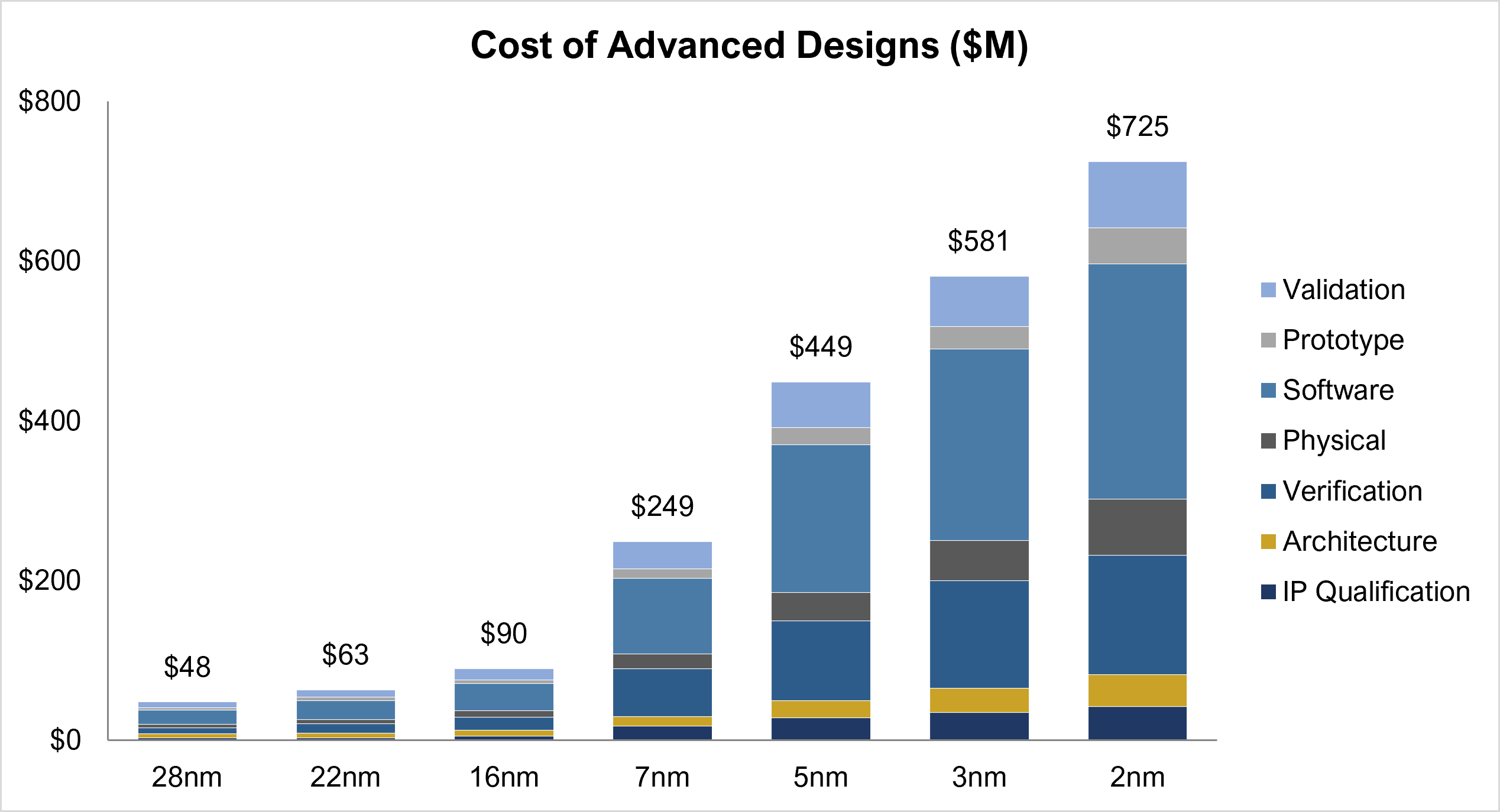
Every leap to a smaller geometry multiplies the verification, physical, and software effort - and a large slice of that incremental spend flows to EDA and IP vendors, because the only way to manage the new complexity is with better tools.
This explains much of the beauty of the EDA business - and why these companies often trade at higher multiples than most semiconductor stocks, in addition to being far less capital-intensive.
EDA vendors aren’t exposed to the violent unit cycles of the semiconductor industry. They sell design capability, and design activity continues to rise even when chip volumes weaken, as AI, automotive, and custom silicon drive a growing number of distinct chip designs.
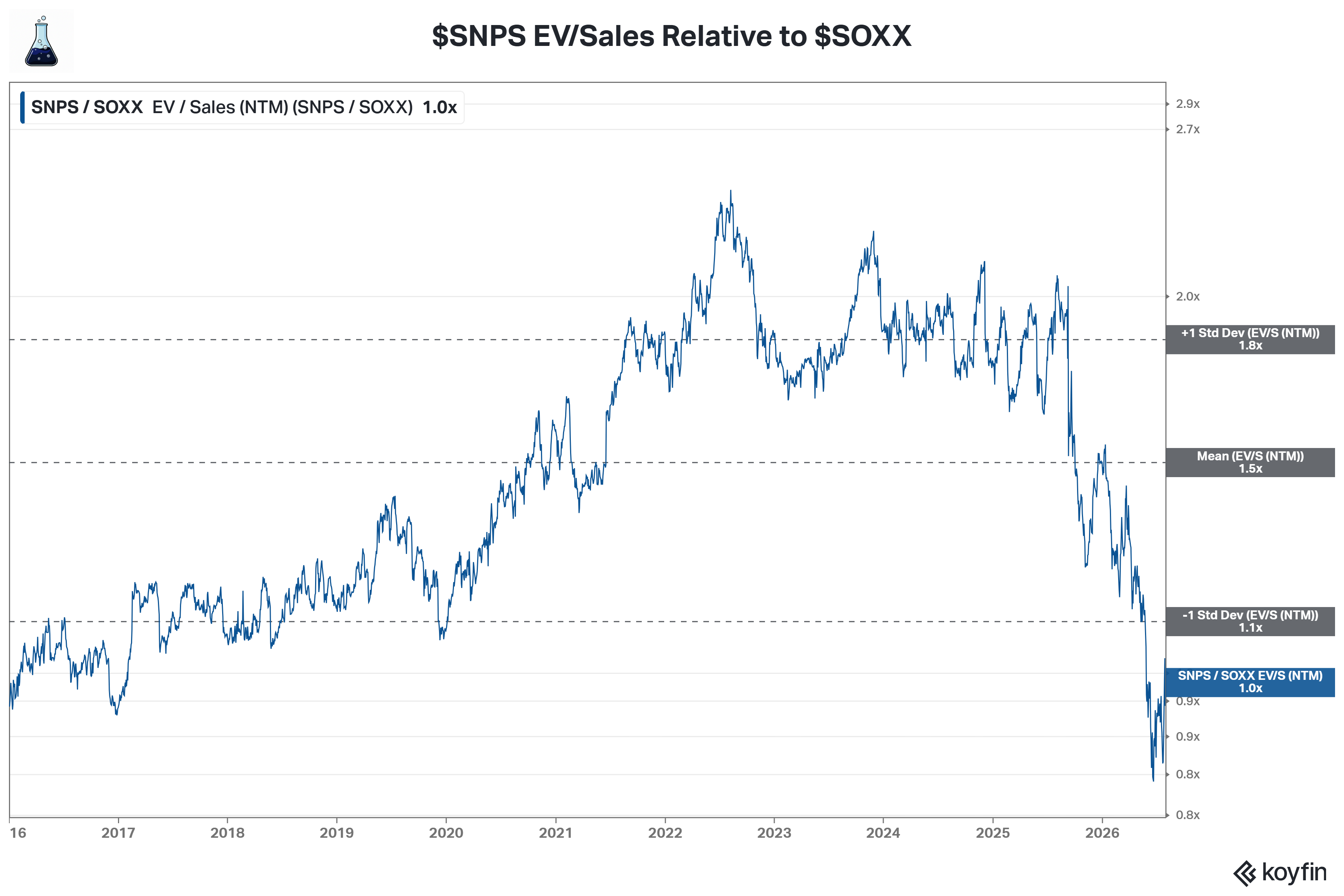
In the chart below, I compare $SNPS’s valuation - measured by its EV/Sales multiple - with that of $SOXX over the past 10 years. Today, $SNPS’s premium is the lowest it has been over the entire period, sitting more than one standard deviation below the historical average.
It’s important to note, however, that the largest tailwind of the past 10 years - the node-on-node cost jumps - is beginning to moderate.
The biggest percentage jumps came at 7nm, when costs rose by +177%, and at 5nm, with an additional +80% increase, largely driven by the transition to EUV lithography. According to IBS, the increases at 3nm and 2nm should be more moderate, at 29% and 25%, respectively.
But while this tailwind is slowing, the runway remains quite long for two main reasons:
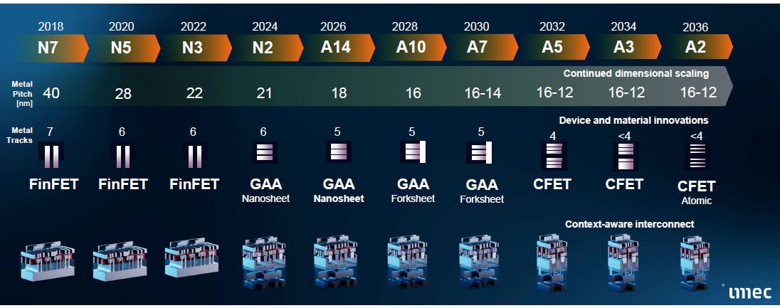
EDA revenue tends to track semiconductor R&D spending, which in turn rises alongside transistor counts and overall chip complexity. And the transistor roadmap still stretches more than a decade into the future, through gate-all-around (GAA) structures and eventually CFET architectures. Imec’s roadmap, for example, extends all the way to the A2 node around 2036.
Second, the number of distinct chip designs (ASICs and others) continues to grow as AI, automotive, industrial applications, and custom silicon developed by hyperscalers become more widespread.
More design starts, each one more complex than the last, create a powerful volume-vs-price tailwind - even as the increase in cost from one node to the next begins to cool.
Found this content valuable? Share it with your network! Help others discover these insights by sharing the newsletter. Your support makes all the difference!
2. Business History:
With the broader industry context now clear, we can turn our attention to Synopsys itself.
The company was founded in 1986 by Aart de Geus, alongside David Gregory, Bill Krieger, and Alberto Sangiovanni-Vincentelli. Most of them had previously worked together at GE’s Advanced Computer-Aided Engineering group in Research Triangle Park, North Carolina.
Originally called Optimal Solutions, the company was built around a then-radical idea: instead of drawing every logic gate by hand, engineers could describe what a circuit was supposed to do and let software generate the gate-level implementation.
In other words, the founding vision was to commercialize logic synthesis, the exact stage of the chip-design flow we discussed earlier.
Synopsys IPO’ed in 1992 and spent much of the following decades expanding beyond synthesis - its flagship product has always been Design Compiler - and into nearly every major stage of chip design through a long series of acquisitions:
EPIC Design Technology (1997): strengthened Synopsys’ position in timing and power analysis.
Avant! (2002): added the physical-design and place-and-route capabilities the company had been missing, helping transform Synopsys from a front-end synthesis vendor into a broader, full-flow EDA platform. The acquisition followed years of litigation between the two companies.
Magma Design Automation (2012): expanded into physical-implementation capabilities and absorbed one of its last major independent competitors in the category.
In 2024, as part of a broader portfolio optimization effort, $SNPS sold its Software Integrity business, effectively exiting an application-security category that never fit naturally within its broader silicon-to-systems strategy.
That same year, the company announced its largest and most ambitious transaction yet: the acquisition of Ansys, which was ultimately completed in July 2025.
Ansys is widely regarded as one of the crown jewels of engineering simulation. Its software allows engineers to build virtual models, predict how products will behave in the real world, and test different design scenarios before committing to expensive physical prototypes.
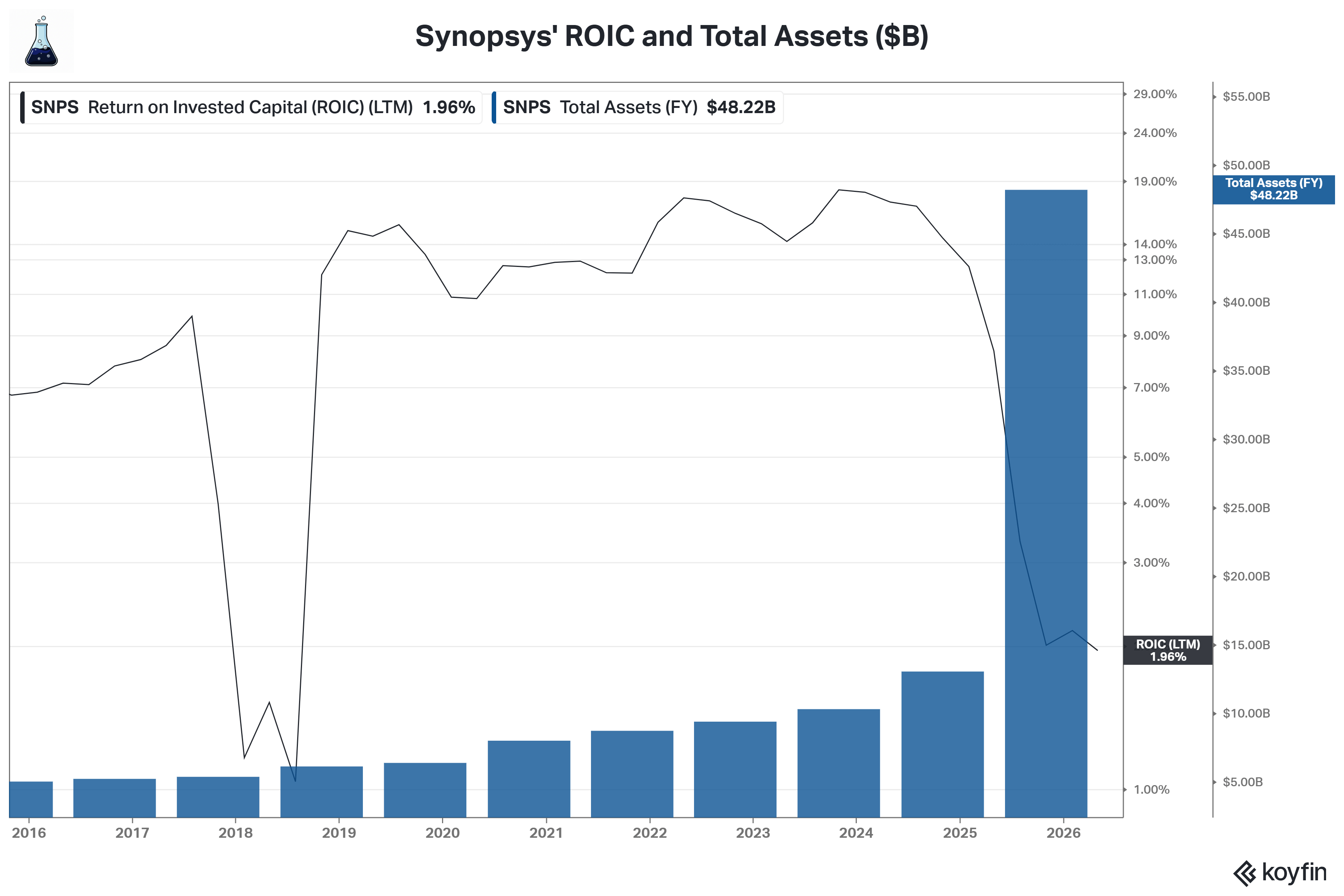
We will discuss Ansys in greater detail in Section 8. For now, take a look at Synopsys’ post-acquisition balance sheet to get a sense of the sheer scale of the transaction.
It is also worth noting that, after 30 years as CEO, Aart de Geus handed the role to Sassine Ghazi in January 2024 and became Executive Chair. Ghazi is a Synopsys veteran who joined the company in 1998 as an applications engineer and gradually rose through the ranks, eventually leading the EDA business before serving as Chief Operating Officer (COO) and, later, President.